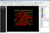
PCB Creator 2.0
Easily design 2 to 4 layer printed circuit boards with up to 1000 pins. PCB Creator is based on professional PCB Design software and is very easy to use. You will have your circuit designed and ready for manufacturing in no time.
Product Specifications
| User Rating: | item has less then 1 vote |
|
| FileCart Rating | Not yet Rated | |
| Submitted by: | bayareacircuits | |
| Homepage | Visit Homepage | |
| License | Freeware | |
| Expires | Days | |
| Price | $0.00 | |
| Downloads | 540 | |
| OS Support | Windows Install and Uninstall | |
| File Name | pcbcreator.exe | |
| File Size | 56.11 MB ( 57,458 KB ) | |
| Published | Oct 31, 2012 (13 years ago) | |
| Updated | Dec 17, 2013 (12 years ago) | |
Follow Us!
Latest Searches
What does an engaged employee tend to do?highlight=0 2 minutes ago
Where to buy BTC on Qwen app 4 minutes ago
does 70 euro per day is only for food in morocco visa application 7 minutes ago
vitamine.jsp?id=51...60 8 minutes ago
nvidia high definition audio treiber windows 11 12 minutes ago
cloud matcha zus 15 minutes ago
nvdidia app 15 minutes ago
Jucatori noi la poli iasi 15 minutes ago
Scientists completely changed their thinking about geology when they discovered….Question 1Select one:a.Continentsb.Plate Tectonicsc.Mountainsd.Climate patterns 17 minutes ago
Popular Searches
id cards 602 times
2025 452 times
2024 385 times
Softperfect 324 times
Database Workbench Pro 258 times
TeraByte Drive Image Backup and Restore 255 times
Elcomsoft Phone Breaker 251 times
ia que faz video com imagem 18 244 times
2026 237 times
Product Details
Easily design 2 to 4 layer printed circuit boards with up to 1000 pins. PCB Creator is based on professional PCB Design software and is very easy to use. You will have your circuit designed and ready for manufacturing in no time. Make your schematic first in the easy to use schematic designer. Choose from a large library of parts and footprints to get exactly what you need. Then convert to PCB to complete the layout with traces, text and more.
After converting Schematic to PCB layout, place board outline and arrange components. Then use placement by list for chips/connectors and auto-placement for other components to get acceptable result in a few minutes and start routing.
PCB Creator PCB software includes 2 automatic routers (Shape-based and Grid-based). Shape Router is able to route complex layouts with SMD components as well as single-layer boards. Grid Router can also make single-layer boards with jumper wires. With Specctra DSN/SES interface you can use external shape-based or topological autorouter. Intelligent manual routing tools allow you to create and edit traces by 90, 45 degree or without any limitations. Curved traces are supported. Through, blind or buried vias can be used in automatic and manual routing. Board size is not limited.
Powerful copper pour system can help to reduce your manufacturing costs by minimizing the amount of etching solution required. To use it, all you have to do is insert a copper area on your board in the PCB Layout program and any pad or trace inside the selected area will be automatically surrounded with a gap of the desired size. Using copper pour you can also create planes and connect them to pads and vias (different thermal types are supported).
Schematic and PCB design modules have number of verification features that help control project accuracy on different design stages: The DRC function shows possible errors in Schematic pin connections using defined rules and allows you to correct errors step-by-step
| Requirements: | Windows Operating System, 1GB Ram, P4 Processor, 100MB HD Space |
| Release Info: | Major Update on Jan 23, 2013 |
| Release Notes: | Updated user interface and order processes |
| Related Tags: | PCB Design PCB Layout PCB Schematics |
Reviews
You must be logged in to write a review
Reviews of PCB Creator 2.0
You can be the first to write a review of PCB Creator!